|
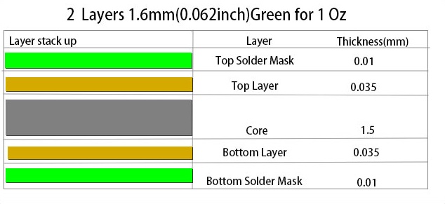
| Fig.1, thanks to Ourpcb.com a design of 2 layers PCB with standard thickness. |
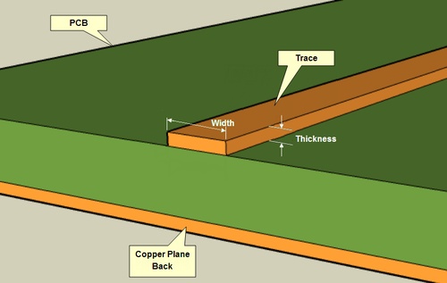
Copper is not a superconductor and too many engineers appear to think it is! Given the length Z, the width X, and the thickness Y of copper can be calculate the resistance R of a copper path.
Every engineer is familiar with resistors, although perhaps fewer are aware of their idiosyncrasies. But too few engineers consider that all the wires and PCB traces with which their systems and circuits are assembled are also resistors. In higher-precision systems, even these trace resistances and simple wire interconnections can have degrading effects. (citation from PCBway)
We must thank Wikipedia for those description: Development of the methods used in modern printed circuit boards started early in the 20th century. In 1903, a German inventor, Albert Hanson, described flat foil conductors laminated to an insulating board, in multiple layers. Thomas Edison experimented with chemical methods of plating conductors onto linen paper in 1904.
Arthur Berry in 1913 patented a print-and-etch method in the UK, and in the United States Max Schoop obtained a patent to flame-spray metal onto a board through a patterned mask. Charles Ducas in 1927 patented a method of electroplating circuit patterns.
The Austrian engineer Paul Eisler invented the printed circuit as part of a radio set while working in the UK around 1936. In 1941 a multi-layer printed circuit was used in German magnetic influence naval mines. Around 1943 the USA began to use the technology on a large scale to make proximity fuzes for use in World War II.
After the war, in 1948, the USA released the invention for commercial use. Printed circuits did not become commonplace in consumer electronics until the mid-1950s.
Even as circuit boards became available, the point-to-point chassis construction method remained in common use in industry (such as TV and hi-fi sets) into at least the late 1960s.
Today to see a modern PCB we must open a modern DSLR or a top quality AMD/nVidia video card.
With graphical analysis we like to measure the trace width of some Printed Circuit Board (PCB), first for amplifier and after for crossover.
In the analysis we only consider the power supply paths and the power lines paths of the amplifiers and crossovers. The ground paths and the heart plane are not analyzed here (they that must be enormous to minimize their resistance).
To better describe "the problem" the photo of some PCB permits us to evaluate it. Below a PCB for DIY construction of an amplifier with (stated) 100W
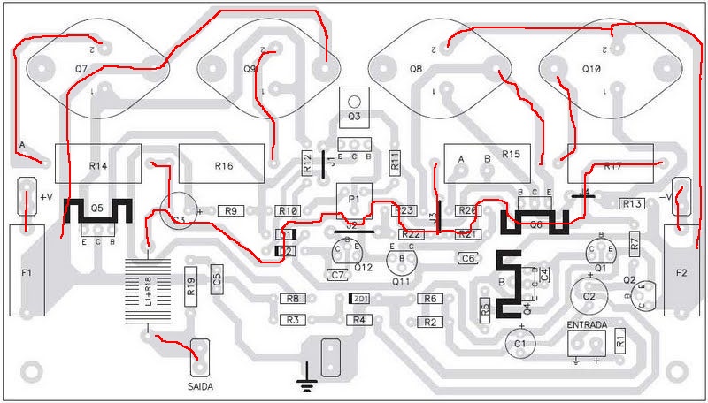 |
| Fig.2, the PCB of an amplifier acclaimed to 100W, in red the path of the power lines and the path of output signal. Using mouse-over we can see the width of traces in mm. For A=2.86mm, in B=2.6mm, in C=1.67mm |
One other PCB to build DIY an amplifier with 150W. Similar design, different schematics, but "better" PCB design.
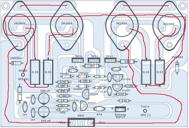 |
| Fig.3, one other PCB also for 150W, in red the path of the power lines and the path of output signal. Using mouse-over in green the trace width in mm. For A=10.2mm, in B=9.4mm, in C=6.7mm, in D=4.5mm |
Acclaimed by producer for 100W, an amplifier with Toshiba transistor probably used a schematics of famous UK amp. Doing the same graphical analysis.
 |
| Fig.4, this PCB for 100W, in red the path of the power lines and the path of output signal. Using mouse-over in green the trace width in mm. For A=3.8mm, in B=3.4mm, in C=3.0mm, in D=2.4mm |
OK, but if I buy a top brand, a real expensive amplifier and top-of-range speakers, this is not a problem for me. Probably all readers think after reading the first part of the analysis.
This is not true, some best brands are poor in the PCB drawing, some PCBs are ridiculous, some have such an ugly design. The width/thickness of the trace is not a problem present in the designer's mind today.
As usual there are excellent exceptions.
From Wikipedia; The LS3/5A is a commercially produced loudspeaker driven by the need of the BBC to monitor and assess broadcast programme quality. It was derived from the LS3/5, which was conceived and developed by the BBC Engineering Department in the early 1970s, Production began in 1975.
-ls35a.jpg) |
| Fig.5, from the datasheet of B110 and from a photo of early LS3/5A we can obtain a measure of the crossover. With mouse-over see the B110 draving |
Next a moder reproduction, accurate, of early version of Rogers (really Swisstone) crossover PCB, the FL6/23 15 ohm version.
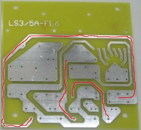 |
| Fig.6, copy of early, original crossover PCB for BBC's LS3/5A. With br>mouse-over in green the trace width, A=4.0 mm, B=3.28 mm, C=2.9 mm, D=2.55 mm |
OK, but I have a modern speaker, designed in 1990 not in 1975, a famous NAIM SBL with mass damper.
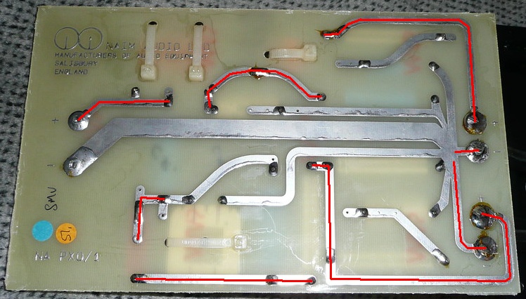 |
| Fig.7, original NAIM SBL crossover PCB, model NA PX0/1, in red the current path Using Mouse-over in green the trace width, A=3.75 mm, B=3.46 mm, C=2.88 mm |
Only 2 other examples, the Tannoy Monitor Gold, the Tannoy HPD 385 and Tannoy Super Red Monitor use the same crossover, only small difference in values, the following
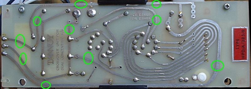 |
| Fig.8, original Tannoy crossover PCB for HPD385 and similar 15', a disaster, see the green circles on the small width traces, practically all are too thin! |
Finally a legend of speaker design, Sir Irving M. Fried, of IMF and TDL. Here the crossover of TDL Studio 4 (but RSTL and all IMF are similar), all suffering the same problem.
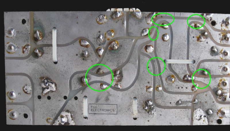 |
| Fig.9, my original TDL Monitor Studio 4 crossover PCB with green circles on the small width traces |
Various calculators can be found online to find the impedance of a PCB track or the cross section required to carry a given current, one interesting is this one.
Let us now have a few calculations to obtain the value of the track section from Fig.2 up to Fig. 9, all in mm2.
 |
| Fig.10, an example of PCB, see also fig.1 for multilayer |
There are a whole series of international norms, and also of use conventions, for the shape, thickness, number of layers, distances between the tracks for PCBs. Below is a table of the most common thicknesses.
| oz/ft2 | 0.5 | 1 | 2 | 5 | 8 |
| inch | 0.000685 | 0.00137 | 0.00274 | 0.00685 | 0.01096 |
| mils | 0.685 | 1.37 | 2.74 | 6.85 | 10.96 |
| mm | 0.0174 | 0.0348 | 0.0696 | 0.1740 | 0.2784 |
| µm | 17.4 | 34.8 | 69.6 | 173.99 | 278.38 |
As described in Fig.1 the standard copper layer have a thickness of about 0.035 mm (stated as 1 Oz/ft2). Reading Fig.10 we can consider the section of trace rectangular and having the width is easy obtain the area section. See below table.
| trace | Fig.2 | Fig.3 | Fig.4 | Fig.6 | Fig.7 | Fig.2 | Fig.3 | Fig.4 | Fig.6 | Fig.7 | |
| A | 0.100 | 0.357 | 0.131 | 0.140 | 0.131 | 0.199 | 0.713 | 0.262 | 0.279 | 0.261 | |
| B | 0.091 | 0.233 | 0.118 | 0.114 | 0.121 | 0.183 | 0.465 | 0.236 | 0.229 | 0.241 | |
| C | 0.058 | 0.202 | 0.105 | 0.102 | 0.100 | 0.116 | 0.403 | 0.210 | 0.203 | 0.201 | |
| D | . | 0.155 | 0.085 | 0.089 | . | . | 0.310 | 0.170 | 0.178 | . |
As comparison we can measure a human hair, chestnut, not blonde of black, with electronic microscope and from diameter calculate the area section, below.
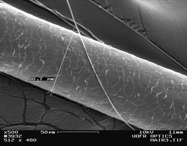 |
| Fig.11, 0.0807 mm for diameter, 0.005115 mm2 for area section thanks to Dr. Luce Scholl, University of Rochester, Institute of Optics, 2007 |
Behind the red binding post of LS3/5A there is a trace (25 cm long) of 0.102 mm2, even behind the red banana port of Naim SBL there is a trace, 3 cm long, of 0.121 mm2, as comparison your hair, chestnut, has a section of 0.005115 mm2.
And the power amplifiers are even worse, circulating currents of dozens of ampere on traces of ridiculous sections. Let's look at the track on the lower left side of Fig.3 (positive power), here marked as A, it seems beautiful big is true? NO, not true, 0.357 mm2.
After opening preamplifier, amplifier, speaker, CD player, turntable for about 40 years I find some tentative of solution of the problem:
 |
| Fig.12, some Bus-Bar. Have you ever seen such a thing on a HiFi amplifier? I NEVER in many years. You can see them on many industrial equipment that cost half or a tenth of our toys! Use mouse-over |
Cables?
Surely we all have PCBs in our amplifiers or crossovers like the ones shown here, they could be greatly improved with the technique f) described above with patience and care in soldering.
 |
| Fig.13, example of audio cables, from dead DCCA Audio and using mouse-over one other probably from Russian Stealth Audio |
But if nothing is done to improve the PCBs, explain to me why buy one of the cables in the photo above (excellent brand) together with other power/speaker cables costing 1000 or 20000 euros per meter?
Donations if you have a Bitcoin wallet
If you have a nice fat wallet you can send a few cents to this code 1ETv1mJTZTB7EiXwZkucF2BTA512Rkaw6 maybe with a message (be careful to the transaction cost, send 0.1 and pay 0.01 is not a good idea).
1ETv1mJTZTB7EiXwZkucF2BTA512Rkaw6 <== my code , Thank you.
Donations if you have not a Bitcoin wallet
If you like this work and measures you can make a small donation of Bitcoin. You do not need a wallet to make a donation, indeed even those who have Bitcoin wallet is better to pass for a web site that "gift" currency since this does not have a transaction cost.
To make a donation you must use some of your web-time on a Bitcoin Faucet, please go to Koiniom.com, enter my code 1ETv1mJTZTB7EiXwZkucF2BTA512Rkaw6 into empty cell and press "Get Free Crypto", a new sub-page appear, do not touch other then the last 2 buttons in lower right corner "Surf Ads" and "Active Window Ads".
If appear a tweet asking to register use the lower right corner button "Close", solve the Captcha and proceed. Of course any next page if different but I suggest you to stay more time possible reading pages and advertisement to produce Bitcoin (1/100000 I suppose) for me.
Be careful, do not use roulette, dices, casino and other stealing web site, as claim of supposed infection. We use Kaspersky Free Antivirus by 2 years without problems.
1ETv1mJTZTB7EiXwZkucF2BTA512Rkaw6 <== my code , Thank you.
| In the last years at Universita' Degli Studi di Roma La Sapienza |
Dr. G. Visco already contract professor for Chemistry in Environment & Cultural Heritage into --> |
Corso di Laurea in: Scienze Applicate ai Beni Culturali ed alla Diagnostica per la loro Conservazione |